

Microwave plasma chip unsealing equipment
Key words: standard leak | MPCVD | capacitance film gauge vacuum gauge | high and low vacuum calibration device | helium leak calibration device
Classification:
Product Details
Chip unsealing is also called unsealing, opening cover and opening cap. In the process of unsealing, the lower filler (the main component is epoxy resin) in the interconnection structure is mainly removed, so that the wire bonding or the chip itself is completely exposed. The schematic diagram of epoxy resin material packaging chip is shown in fig. 3. the unsealing process requires local corrosion of the completely packaged IC to expose it, while keeping the chip function intact, keeping die, bond pads, bond wires and even lead-undamaged, and Au, Cu or Ag leads undamaged.
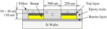
Figure 3 Schematic diagram of epoxy resin encapsulated chip
The microwave plasma method has developed special equipment for microwave plasma etching for various types of semiconductor devices, as shown in Figure 4. Microwave plasma etching equipment has the advantages of high energy density, good etching effect, fast etching rate, and various protective gases. It is suitable for rapid etching and unsealing of epoxy resin and silicon-based mixed materials. At the same time, Au and Cu leads can be effectively protected under pure O environment, and Ag leads can be effectively protected by H2, thus meeting the high efficiency etching of various metal lead chips.
plasma opening
The opening process does not cause damage to retain surface features.
Retain the original contamination impurities and failure points
chemical opening
Will reduce the wire diameter will reduce the mechanical strength
Can corrode copper wires and aluminum pads
plasma opening
Only use hydrogen and oxygen formula, the chip damage is small and the opening time is reduced by 80%.
Fully automatic opening process
Retain the original contamination impurities and regular air pressure at the point of failure, reducing repair and maintenance costs
Traditional plasma opening
CF4 etching can cause damage to the passivation layer and chip
Although CF4 is added, the opening time is still long.
Manual cleaning of inorganic impurities from each etching step
May cause original contamination impurities and failure points to be eliminated
Vacuum system, repair and maintenance costs are higher
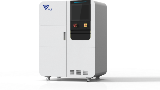
Fig.4 Microwave plasma etching equipment
Epoxy resin and silicon mixed material packaging chip is etched and unsealed by microwave plasma etching equipment. The surface morphology of the chip before unsealing is shown in Figure 5 (after laser unsealing). It can be seen that the chip bonding Cu lead has been coated by the packaging material. The packaged chip is etched in pure O low pressure environment. The chip morphology after etching and unsealing is shown in Figure 6. The epoxy resin packaging material on the chip surface has been all etched by microwave plasma, and the bonding material Cu lead is not damaged, and the clear structure of the chip surface can be seen after etching. Therefore, microwave plasma etching is suitable for efficient, stable and non-destructive opening of semiconductor chips.
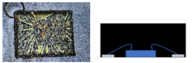
Fig.5 Schematic diagram of surface morphology and section of unopened chip
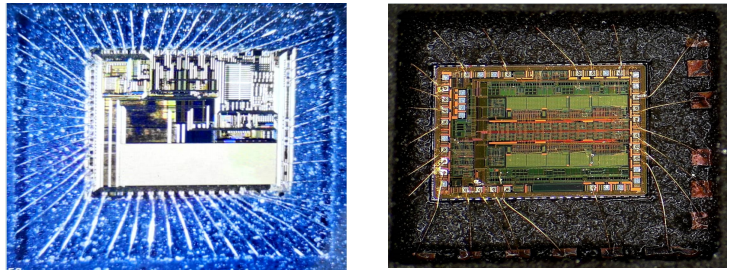
Fig.6 Schematic diagram of chip surface morphology and cross section after microwave plasma etching
Application of Failure Analysis and Quality Control
1. Wire bond:
⚫Silver wire (Ag)
⚫Copper wire, composite cementitious material, gold wire, aluminum wire (Cu,PCC,Au,Al)
⚫regular or aging-tested samples
2, flip chip (Flip Chip)
⚫Rewiring Layer (RDL)
⚫Cu Pillar, Solder Bump
⚫Fan-in and Fan-out WLP
3, the chip.
⚫ BOAC
⚫ SAW、BAW
⚫Gallium arsenide chip, gallium nitride chip GaAs,GaN
4. Encapsulation
⚫ 2.5D / 3D
⚫ SiP、CoWoS
⚫ Chip on Board
5. Packaging materials
⚫ High Tg
⚫ Glob Top
⚫ Underfill、DAF、FOW
⚫ Clear Mold, Die Coat
6. FA Type
⚫Electrical overstress (EOS)
⚫Migration (Migration)
⚫Corrosion (Corrosion)
⚫Impurity contamination (Contamination)
Related Products
Product inquiry
Address
9959 Songze Avenue, Qingpu District, Shanghai
WeChat Sweep
Follow our official WeChat